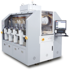
STW-10 automated plasma system is designed for front-end semiconductor processing. It is especially well suited for activating silicon surfaces prior to hybrid wafer bonding. The STW-10 accepts FOUP’s containing 300mm wafers, or cassettes with dies on tape frame. Maximum throughput is 60 wafers per hour. Inside the STW-10, the Atomo™ plasma system generates a uniform, particle-free, electrically neutral discharge that will not damage CMOS integrated circuits.

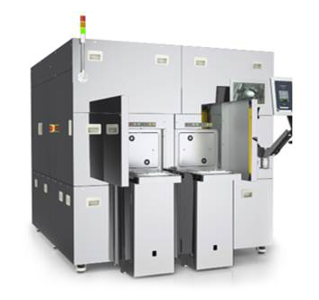
STW 10

STW-10 automated plasma system is designed for front-end semiconductor processing. It is especially well suited for activating silicon surfaces prior to hybrid wafer bonding. The STW-10 accepts FOUP’s containing 300mm wafers, or cassettes with dies on tape frame. Maximum throughput is 60 wafers per hour. Inside the STW-10, the Atomo™ plasma system generates a uniform, particle-free, electrically neutral discharge that will not damage CMOS integrated circuits.

Category:

TECHNICAL DOCUMENTS

Leave a Reply

Your email address will not be published. Required fields are marked *